Minuscule silicon chiplets: a new level of micro manufacturing
Updated: 2013-04-21 07:50
By John Markoff(The New York Times)
|
|||||||
|
Tiny chiplets no larger than a grain of sand are suspended in a solution that can be printed onto surfaces. Amy Sullivan / PARC |
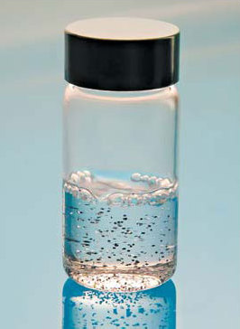
PALO ALTO, California - Under a microscope, four slivers of silicon - electronic circuits called chiplets - perform an elaborate, jerky dance as if controlled by a hidden puppet master. Then on command, they all settle with pinpoint accuracy, precisely touching a pattern of circuit wires, each at just the right point of contact.
The technology, on display at Xerox's Palo Alto Research Center, or PARC, is part of a new system for making electronics, one that takes advantage of a Xerox invention from the 1970s: the laser printer.
If perfected, it could lead to desktop manufacturing plants that "print" the circuitry for a wide array of electronic devices - flexible smartphones that won't break when you sit on them; a supple, pressure-sensitive skin for a new breed of robot hands; smart-sensing medical bandages that could capture health data and then be thrown away.
Today's chips are made on large wafers that hold hundreds of fingernail-sized dies, each with the same electronic circuit. The wafers are cut into individual dies and packaged separately, only to be reassembled on printed circuit boards, which may each hold dozens or hundreds of chips.
The PARC researchers have a very different model in mind. With financing from the National Science Foundation and from Darpa, the Pentagon's Defense Advanced Research Projects Agency, they have designed a laser-printer-like machine that will place tens or even hundreds of thousands of chiplets, each no larger than a grain of sand, on a surface in exactly the right location and in the right orientation.
The chiplets can be both microprocessors and computer memory as well as the other circuits needed to create complete computers.
The new manufacturing system the PARC researchers envision could be used to build custom computers, or as part of a 3-D printing system that makes smart objects with computing woven into them.
The researchers are years from placing tens or hundreds of thousands of circuits accurately in a fraction of a second. And they acknowledge that this would be only the first step in designing a commercially viable system.
The research could have tremendous economic consequences - feeding the emergence of a new digital era in manufacturing, much as laser printing transformed publishing three decades ago.
Eugene Chow is an electrical engineer who leads the PARC team that has designed the new technology, which they have dubbed "Xerographic micro-assembly." The technology breaks silicon wafers into tens of thousands of chiplets, bottles them as "ink" and then "prints" them, much as a Xerox laser printer puts toner on paper.
"It's a crazy new revolutionary tool," he said.
Already, more than half a dozen different printing techniques, from inkjet to gravure to offset printing, have been used to make electronic circuits - a business that was estimated at $9.4 billion last year.
But the PARC researchers argue that all of the current commercialized techniques are limited in that they can't achieve the transistor density now available through conventional chip manufacturing. So while it is possible to use printing techniques to make a flexible display screen with hundreds or even thousands, of transistors, it cannot be done with millions or billions of transistors, like today's silicon chips.
The new PARC technology is intended to address that shortcoming and bridge the two worlds by smearing computing power across areas much larger than today's postage stamp-sized chips.
Greg Whiting, a senior research scientist at PARC, said, "This is a very different way to think about electronics."
The New York Times
(China Daily 04/21/2013 page11)