Samsung expands global footprint
|
An artist's rendering of Samsung Semiconductor's future American headquarters in San Jose, California. Provided to China Daily |
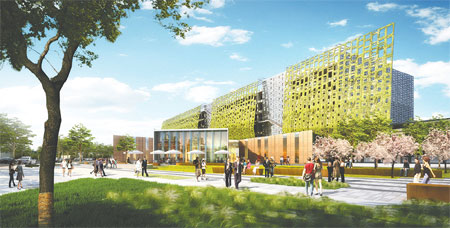
Samsung Electronics had a ground-breaking ceremony in San Jose, California on July 10 for its new North American headquarters. The 10-story, $300 million facility, featuring 1.1 million square feet of floor space, will be open for operation by the summer of 2015.
"It's a magnificent day for Silicon Valley," said Mike Rossi, a senior advisor to California governor Jerry Brown. "And this would not have happened without the great teamwork of the governor's office, Santa Clara County, the City of San Jose, and Samsung all working together."
Just 11 days ago, South Korean president Park Geun-hye, visited Xi'an, where Samsung launched its US$7 billion, high-end memory chip project in September 2012. The project marked Samsung's biggest overseas investment to date, as well as the largest electronics project in China's Midwest region.
Zhang Baotong, director of the Regional Development Advisory Center of the Shaanxi Provincial Academy of Social Sciences, said Samsung's investment brings a cluster of electronic components makers, which will have a long-term impact on Xi'an and Shaanxi's economic development.
In San Jose this week, Charlie Bae, president of Samsung Semiconductor Inc, said the company will continue to lead its device solution businesses in North America by pursuing high quality market solutions, primarily focused on providing components that enhance the worlds of television, smart phones, tablets, PCs, home appliances, semiconductors and LED products.
"Consumers and their digital devices have become inseparable, as the number of people using such devices and the frequency of usage continues to skyrocket," said Jim Elliott, vice-president of Samsung Semiconductor Inc. "Enabling this growth is the increasing sophistication of the components contained in the devices."
And Samsung is probably the largest producer of those components, which include displays, memory, processors and storage media, Elliott said.
"We're outgrowing our facilities in many areas," Elliott said. "This is probably most evident here in Silicon Valley, where we now have big plans for the future."
The site will house several cutting-edge research labs, as well as sales and marketing staff.
Chuck Reed, mayor of San Jose, praised Samsung's contribution to Silicon Valley and the city of San Jose.
"It's because of companies like Samsung that choose to stay in the valley and our city, that we have new jobs created everyday, which makes Silicon Valley one of the most desirable places for international talent to stay and work, no matter where they come from," said Reed. "Silicon Valley continues to be the leading choice for venture capitalists, a cradle for world talent and high paying jobs to grow California economy."
Jonathan Ward, partner at NBBJ, the architectural firm that designed the new building, said it took his team approximately 10 months to complete the plan.
"We had worked with Samsung in Seoul before (Samsung International Hospital), and we are proud of the outcome of that state-of-art project," said Ward.
Ward said the new building will be clad in white metal and clear glass in a way that reduces solar heat gain. The campus also will include a star-shaped cafeteria, rain gardens, basketball courts, and a spacious parking garage. There will be "fresh air" outdoor space on two of the above-ground floors to add to the open style of the facilities, allowing employees to be outdoors while inside the building.
Samsung's Xi'an facility is expected to become fully operational by the end of 2013, when it will have a monthly output of 100,000 chips and annual sales of 66 billion yuan ($10.4 billion).
This biggest ever overseas investment is located in Xi'an Hi-tech Industrial Development Zone and will produce nanometer chips, mainly for use in smartphones and tablet PCs.
Xi'an Mayor Dong Jun said the city government provided an area of 9.2 square kilometers for the Samsung project and the supporting service infrastructures to ensure its success.